Tips for Reducing EMI in PCB Designs
EMI is everywhere. Without the proper precautions, it can wreak havoc on your devices, including your PCB. EMI, or electromagnetic interference, is electromagnetic energy that disrupts the signaling in an electronic device through radiation or induction. It doesn’t take much to create EMI. All you need is energy and an antenna. All electronic devices create EMI, and all electronic devices can be affected by it—but there are ways to mitigate its effects. Mitigating EMI starts with the design of your PCB. Let’s check out some tips for reducing EMI in PCB designs, so you can stop EMI in its tracks.
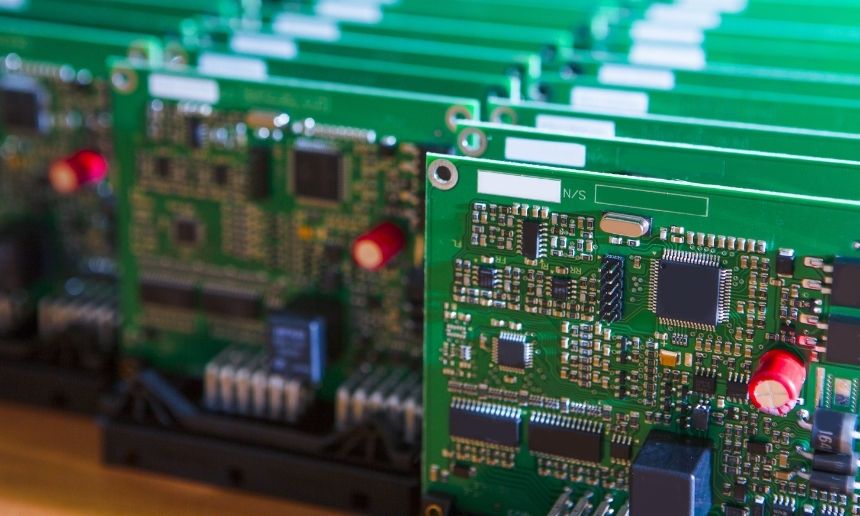
The Ground Plane
A ground plane is an electrically conductive surface that connects to electrical ground. In PCBs, the ground plane is an area of copper foil. It connects to the power supply ground terminal and acts as a return path for current from different components on the board. The bigger the ground plane, the less you’ll have to deal with electrical noise, interference through ground loops, and crosstalk. When the digital circuits switch state, current pulses will flow from the active devices into the ground circuit. A high impedance will lead to a voltage drop, which can result in significant noise. By providing a larger conducting area, you can cut down on interference. Other methods for optimizing your ground plane include:
- Using a multi-layer board
- Using split grounds cautiously
- Connecting split ground planes at a single point
- Connecting bypass or decoupling capacitors to the ground plane
The Trace Layout
Another tip for reducing EMI in PCB designs is to focus on the trace layout. A trace is a conductive path. When a circuit is active, it contains flowing electrons. Crossing or bending the trace layout could lead to the formation of an antenna. When you’re designing your trace layout, make sure to:
- Avoid sharp right-angle bends
- Keep your signals separate
- Keep return paths short
- Isolate high-speed components
- Keep analog circuits separate from digital circuits
EMI Shielding
Most devices produce EMI. To cut down on the negative effects, you’ll want to focus on electromagnetic compatibility, or designing your circuit to prevent disruption by shielding it. By shielding your devices, you can protect your receivers from external electromagnetic signals, or prevent a stronger signal from escaping and interfering with other electronics. An EMI shielding coating can cover vulnerable PCB elements, along with connectors and cables between PCBs.
Using dual-fire or our patented quad-fire vacuum metalization process, Deep Coat can create precise, effective PCB shield designs. If you’re looking for a way to protect your devices against EMI, contact us to discuss our custom PCB EMI shielding services.